|
|
|
| J# J1 J2 J3 J4 J5 J6 J7 J12 J13 J14 J27 J30 J34 J35 J36 J38 |
Type 6-Pin Mini-Din (Female) 6-Pin Mini-Din (Female) 15-Pin High Density D-Shell (Female) 15-Pin D-Shell (Female) 25-Pin D-Shell (Female) 9-Pin D-Shell Connector (Male) 6-Pin 112-Pin MCA 6-Pin 26-Pin (2x13) Header 112-Pin MCA 4-Pin Connector 8-Pin Connector 2-Pin Connector 4-Pin Connector 3-Pin Connector |
Description Jpkb (Keyboard Connector) Jpmo (Mouse Connector) Jvga (VGA Connector) Jgam (GamePort Connector) Jlpt (Parallel Port Connector) Jcom2 (Com Port Connector) Power Connector 1 Riser Connector 1 (ISA Riser Slot) Power Connector 2 Jvesa Riser Connector 2 (VL-BUS Riser Slot) Jbte (External battery connector) Front Panel Jklk (Keyboard lock connector) Jspk (External speaker connector) Jfane |
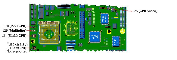
U50 CPU (DX, DX2, DX4, SX, SX2, P24T)
Zero Insertion Force (ZIF) socket. No special tools are required to upgrade the CPU with an Intel Overdrive Processor.
The PB450 motherboard uses 237-pin type 3 CPU socket.
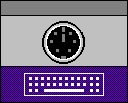
J1 PS/2 Keyboard Port
J1 is a female 6-pin mini DIN connector built-in on the motherboard.
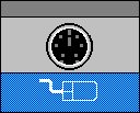
J2 PS/2 Mouse Port
J2 is a female 6-pin mini DIN connector built-in on the motherboard.
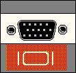
J3 VGA Port
J3 is a female 15-pin DB15 port built-in on the motherboard.
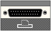
J5 Parallel Port
J5 is a female DB25 parallel port built-in on the motherboard.
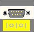
J6 Serial Port
J6 is a male DB9 serial port built-in on the motherboard. The UART type is 16C550 compatible.
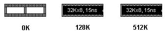
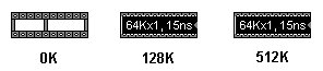
U16,U19,U29,U32 Cache Upgrade Sockets
Cache memory is upgradeable to 128KB or 512KB.
U55 Cache-TAG Ram Socket
U57, U58 Cache-DB Ram Socket
Main Memory Bank
(BANK 0) (U60, U61, U62, U63)
Main memory bank (1M x 4).
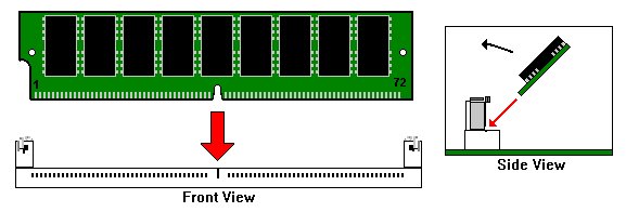
SIMM Sockets (U66 BANK 1 / U73 BANK2)
Use 72 pin SIMMs.
U9 Keyboard Controller
8242 Keyboard Controller
U10 Video Controller Cirrus Logic
CL-GD 5428 or 5429
J14 (JVESA) Video Feature Connector, 26 Pin (2x13)
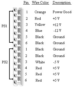
Power Connector (PS1 / PS2)
U14 Super AT I/O Controller
SMC 37C665 floppy, serial and parallel controller.
U8,U49 Programmable Array Logic (PAL)
PAL16L8F25S
U22,U36 Video Memory (1st Megabyte)
2 x 256Kx16 surface mounted chips
U26,U27 ZIP Video Memory Sockets
The PB450 with a CL-5428 chip is upgradeable to 2 MB of video memory by adding two 256Kx16 (symmetrical, CAS line) DRAM ZIPs.
U53 VL-Bus IDE Interface Controller
OPTi 82C611
U46 Data Buffer Controller
OPTi 82602
BT1 On-board Battery
CMOS battery (soldered)
U52 AT Single Chip Controller
OPTi 82C802
U15 BIOS
Flash BIOS 1.1A (latest)
BZ1 On-board Buzzer
Piezoelectric speaker
J39 (RESERVED)
Note
This jumper only exists on the PB450 Rev. G motherboard.
DO NOT CHANGE
J40 (RESERVED)
Note
This jumper only exist on the PB450 Rev. G motherboard.
DO NOT CHANGE
J41 (RESERVED)
Note
This jumper only exist on the PB450 Rev. G motherboard.
DO NOT CHANGE
Note
When two 32MB SIMMS are installed in the SIMM sockets, the SMT memory needs to be disabled. This is done by jumping J37.
Enabled
![]()
Disabled

Default J22 (Jmod) DB Modem Connector
20 Pin (2x10) Header.
J21 (Jfdd) Floppy Drive Connector
34 Pin (2x17) Header.
J23 (Jhdd) Hard Drive Connector
40 Pin (2x20) Header.
J24 (Jhddloc) Local Bus Hard Drive Connector
40 Pin (2x20) Header.
U40,U41 Octal Transparent Latch
74F373
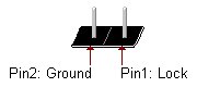
J35 (Jklk) Keylock Connector
J34 Front Panel Connector
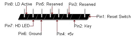
Default
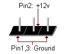
J38 (Jfane) Aux. Fan Connector
U48 Surface-Mount CPU Traces
Some motherboards have a CPU soldered directly into this location. Upgrades are not affected by this CPU. These motherboards are identified by an 'S' in the part description.