|
|
|
| U | Part | Description |
| U13 | E1 | GD75189AD |
| U13 | J1 | empty |
| U12 | A1 | LM317LM |
| U12 | B1 | TLC34076-170FN |
| U12 | D1 | F373 |
| U12 | D2 | ICS2492M |
| U12 | E1 | SN75188 |
| U12 | E2 | 74F243D |
| U12 | F1 | N85C220 |
| U12 | G1 | GD75189AD |
| U12 | G2 | GD75189AD |
| U12 | J1 | empty |
| U11 | A1 | C56D-3B01 |
| U11 | A2 | MLS151 |
| U11 | A3 | LM339A |
| U11 | G2 | F245 |
| U11 | G3 | F244 |
| U10 | A1 | Video ZIP socket |
| U10 | A2 | Video ZIP socket |
| U10 | B1 | Video ZIP socket |
| U10 | B2 | Video ZIP socket |
| U10 | B3 | Video ZIP socket |
| U10 | B4 | Video ZIP socket |
| U10 | B5 | Video ZIP socket |
| U10 | C1 | Video ZIP socket |
| U10 | D1 | MACH32 210688AX00 |
| U10 | G2 | 74HCT14D |
| U10 | G1 | N28F001BX-T120 |
| U10 | J1 | DS12887 |
| U8 | A1 | KM424C2572-6 |
| U8 | A2 | KM424C2572-6 |
| U8 | A3 | KM424C2572-6 |
| U8 | A4 | KM424C2572-6 |
| U8 | B1 | KM424C2572-6 |
| U8 | B2 | KM424C2572-6 |
| U8 | B3 | KM424C2572-6 |
| U8 | B4 | KM424C2572-6 |
| U8 | D1 | RZ1000BP |
| U8 | G1 | FDC37C655QFP |
| 8 | H1 | ALS245A |
| U8 | B1 | ICD2028DSC-ES |
| U8 | C1 | F08 |
| U8 | G1 | S823781B |
| U8 | H1 | ALS245A |
| U6 | B1 | KM68257BJ-15 |
| U6 | B2 | KM68257BJ-15 |
| U6 | C1 | 82433LX |
| U6 | D1 | S82433LX |
| U6 | J1 | F125 |
| U5 | A1 | 74FR244 |
| U5 | B1 | KM68257BJ-15 |
| U5 | B2 | KM68257BJ-15 |
| U5 | F1 | 74F243D |
| U5 | G1 | F00 |
| U5 | H1 | F04 |
| U5 | J1 | 74F32 |
| U5 | J2 | F08 |
| U4 | A1 | KM68257BJ-15 |
| U4 | B1 | KM68257BJ-15 |
| U4 | B2 | KM68257BJ-15 |
| U4 | C1 | KM68257BJ-15 |
| U4 | D1 | S82433LX |
| U4 | F1 | 74F243D |
| U4 | G1 | 74F243D |
| U4 | H1 | 74F243D |
| U4 | H2 | 1MX4 DRAM |
| U4 | J1 | 74F07D |
| U3 | F1 | 74F243D |
| U3 | H1 | F138 |
| U2 | A1 | F373 |
| U2 | A2 | F373 |
| U2 | B1 | CPU SOCKET |
| U2 | D1 | S82434LX |
| U2 | G1 | 74F243D |
| U2 | H1 | F32 |
| U2 | J1 | F125 |
| U2 | J2 | F32 |
| Y | Description | Pin/Setting | Description |
| J 12 H1 RCVR/NRM | Flash Boot Block | 1-2 2-3 | Recovery Mode Normal Mode (default) |
| J 12 H1 PROG/WP | Flash Write Enable/Disable | 4-5 5-6 | Flash Write Enabled (default) Flash Write Protected |
| J 13 H1 CMOS CLR | CMOS Clear | 1-2 2-3 | Normal (default) Clear) |
| J 13 H1 ENA/DIS | Password | 4-5 5-6 | Normal (default) Clear |
| J 13 H3 Mono/Color | VGA Mode | 1-2 2-3 | Monochrome Color (default) |
| J 13 H3 ENA/DIS | VGA Mode | 4-5 5-6 | Enable (default) Disable |
| J 7 A1 66/60 | CPU Speed (this setting cannot be changed) | 1-2 2-3 | 66 MHz 60 MHz (default) |
| Setup | CMOS Setup | 1-2 2-3 | Enable (default) Disable |
| J | Description |
| J1 G3 | HD LED | ||
| J4 H1 | SIMM BANK 0 | ||
| J4 H2 | SIMM BANK 0 | ||
| J4 G1 | SIMM BANK 1 | ||
| J4 F1 | SIMM BANK 1 | ||
| J 7 J1 | IDE2 | ||
| J 8 J1 | FLOPPY | ||
| J 8 J2 | IDE | ||
| J 9 F1 | RISER SLOT | N/A | N/A |
| J 9 H1 | Auxilliary 3.3V Power | ||
| J 10 A1 | VESA | ||
| J 13 H5 | KEYBD | ||
| J 13 G1 | MOUSE | ||
| J 13 A1 | VIDEO | ||
| J 13 E1 | COM2 | ||
| J 13 F1 | COM1 | ||
| J 13 C1 | PARALLEL |
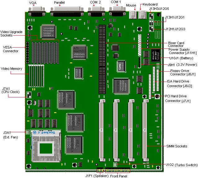
| J13A1 is a female DB15 VGA port built-in on the motherboard. |
J13C1: Parallel Port
| J13C1 is a female DB25 parallel port built-in on the motherboard. |
External Serial Port
| J13E1 and J13F1 is a male DB9 external serial port built-in on the motherboard. J13E1 is COM2. J13F1 is COM1. |
J13G1: PS/2 Mouse Port
| J13G1 is a female 6-pin mini DIN connector built-in on the motherboard. |
J13H5: PS/2 Keyboard Port
| J13H5 is a female 6-pin mini DIN connector built-in on the motherboard. |
J9F1: Riser Card Connector
| The riser card inserted in J9F1 can accommodate up to four 16-bit AT-compatible adapters and two 32-bit PCI adapters, or three 16-bit AT-compatible adapters and three 32-bit PCI adapters at any one time. |
U10J1: Battery
| U10J1 is a Dallas DS12887 real time clock and CMOS battery. |
J8J1: Floppy Drive Interface
| J9H1 is a male 2 x 17-pin floppy drive connector. |
J8J2: ISA Hard Drive Interface
| J9H2 is a male 2 x 20-pin ISA/IDE connector. |
J7J1: PCI Hard Drive Interface
| J9G1 is a male 2 x 20-pin PCI/IDE connector. |
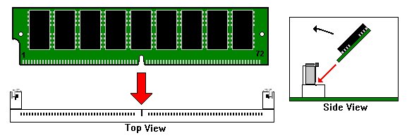
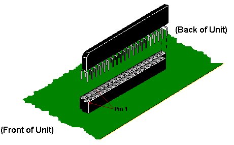
J4F1 thru J4H1: SIMM Sockets
| Uses 1/2/4/8/16/32 MB 72-pin SIMMs, 70ns |
See Also: Ram Upgrade Information Front Panel 
U10G1: Flash BIOS EEPROM
| This is the Flash BIOS EEPROM surface mounted on the motherboard. |
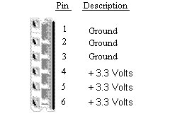
J9H1: PCI Bus Power Connector
| J9H1 is the 3.3V Power Connector for the PCI bus. |
J10A1: Video Feature Connector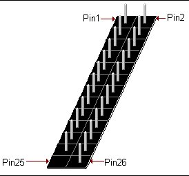
Video Memory Upgrade Sockets
| Video memory can be upgraded to 2 MB by installing eight 256KBx4, 70ns VRAM ZIPs at locations U10C1, U10B5, U10B4, U10B3, U10B2, U10B1, U10A2, and U10A1. |
Also See: Video Upgrade Information Video Memory
| U8A1 and U8B4 make up the 1 MB video memory built-in on the motherboard. |
Also See: Video Upgrade Information Cache Memory
| U4A1 thru U6B2 make up the 256K L2 cache built-in on the motherboard. |
Also See: Cache Upgrade Information U4B2: CPU Socket
| At the moment, this socket can only accommodate the Pentium 60 processor. |
| Uses the 273-pin Type 4 CPU Socket. |
Also See: Cpu Upgrade Information Power Connector (PS1 / PS2)

J1G2: Turbo Switch 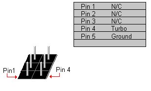
J3A1: External Fan Connector 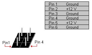
J7A1: CPU Clock 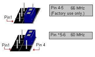
J12H1: Flash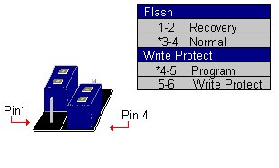
J13H1: CMOS and Password Options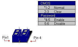
J13H3: Monitor Setting 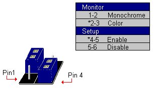
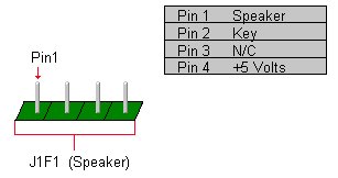
J1F1: Speaker