|
|
|
Note
Installing a video expansion card will automatically disable the on board video controller.
| Sockets | Part |
| AS7C3256-20JC | ||
| 74FCT16373TPV | ||
| KM416C256AJ-6 | ||
| KM416C256AJ-6 | ||
| CPU | ||
| AS7C3256-20JC | ||
| AS7C3256-20JC | ||
| 74FCT16373TPV | ||
| 74FCT16373TPV | ||
| 74FCT16373TPV | ||
| 74FCT16373TPV | ||
| AV9154A-27 | ||
| 412089TF04 | ||
| SOJ DRAM socket | ||
| AS7C3256-20JC | ||
| S82433NX | ||
| VRAM SOCKET | ||
| CL-GD5434 | ||
| S82434NX | ||
| S82433NX | ||
| RZ1000BP | ||
| 74FR244 | ||
| GD75232D | ||
| 74F06D | ||
| 74F245 | ||
| 74F244 | ||
| 74F244 | ||
| 74F244 | ||
| 74F244 | ||
| 74F138D | ||
| 74F08D | ||
| 74F07D | ||
| 74F04 | ||
| S82378ZB | ||
| FDC37C665GT | ||
| N82C42PE | ||
| 74HCT14D | ||
| 74F244 | ||
| 74LS273 | ||
| 28F001BX | ||
| TMS44400DJ-70 | ||
| TMS44400DJ-70 | ||
| 74F244 | ||
| 74F244 | ||
| 74F244 | ||
| 74F244 | ||
| 74F244 | ||
| 74F244 | ||
| 74138D | ||
| 74F125 | ||
| 74F08D | ||
| 74F07D | ||
| ALS245A | ||
| ALS245A | ||
| 74F243D | ||
| DS12887 | ||
| 4011B | ||
| TMS44400DJ-70 | ||
| TMS44400DJ-70 | ||
| 74F244 | ||
| 74F244 | ||
| 74F244 | ||
| 74F244 | ||
| 74F244 | ||
| 74F244 | ||
| 74F32 | ||
| 74F32 | ||
| 74F243D | ||
| 74F125 | ||
| 74F00D | ||
| 431AC |
| J | Description | Pin/Setting | Description |
| J1 J1 (75/90) | CPU Base Speed | 1-2 2-3 |
75MHz Base CPU Speed 90MHz Base CPU Speed |
| J1 J2 (75/90) | Clock Multiplier | 1-2 2-3 |
2x Multiplier 1.5x Multiplier |
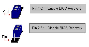
| J1 H1 (RCVR) | Flash Boot Block | 1-2 2-3 (default) | Recovery Mode Normal Mode |
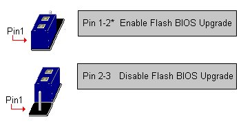
| J1 H2 (PRG) | Flash Write Enable/Disable | 1-2 (default) 2-3 | Flash Write Enabled Flash Write Protected |
| J1H3 (SETUP) | CMOS Setup | 1-2 (default) 2-3 | Enable Disable |
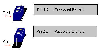
| J1 H4 (PWD) | Password | 1-2 (default) 2-3 | Normal (Enable) Clear (Disable) |
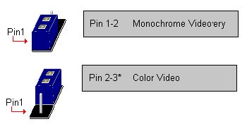
| J1 H5 (MO/CLR) | VGA Mode | 1-2 2-3 (default) | MONO COLOR |
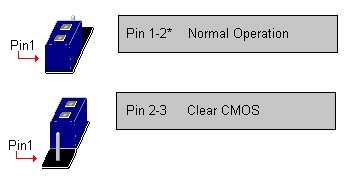
| J1 H6 (CMOS) | CMOS Clear | 1-2 (default) 2-3 | Normal Clear |
| J9 N1 (3.3V) | CPU Voltage Select | 1-2 2-3 | 3.45V 3.3V |
| J | Description |
| J1 N1 VGA Monitor Connector |
| J1 L1 VESA® Feature Connector |
| J3 N1 Parallel Port Connector |
| J5 N1 Serial Port (COM 2) Connector |
| J5 A2 Turbo Switch Connector (Reserved) |
| J5 L1 Auxiliary 3.3V Power Connector |
| J5 D1 SIMM Socket |
| J6 D1 SIMM Socket |
| J6 D2 SIMM Socket |
| J6 N1 Serial Port (COM 1) Connector |
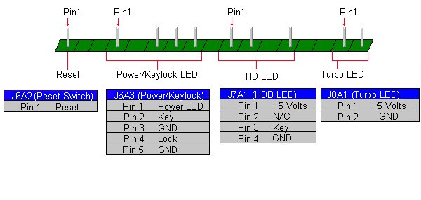
| J6 A1 External Speaker Connector |
| J6 A2 Reset Connector |
| J6 A3 Keylock Connector |
| J7 N1 Mouse Connector |
| J7 D1 SIMM Socket |
| J7 A1 Hard Disk LED Connector |
| J8 J1 Riser Connector |
| J8 N1 Keyboard Connector |
| J8 A1 Turbo LED Connector |
| J8 J1 Daughter Board Connector (COM 1) |
| J9 M1 Primary Power Connector |
| J9 G1 PCI IDE Connector |
| J9 H2 ISA IDE Connector |
| J9 H1 Floppy Connector |
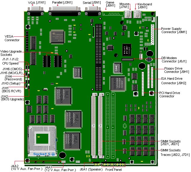
| J1N1 is a female DB15 VGA port built-in on the motherboard. |
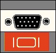 |
| J3N1 is a female DB25 parallel port built-in on the motherboard. |
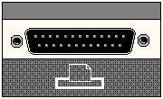 |
| J5N1 is a male DB9 external serial port built-in on the motherboard. |
 |
| This system does not have a built-in game port on the motherboard. |
| J7N1 is a female 6-pin mini DIN connector built-in on the motherboard. |
 |
| J8N1 is a female 6-pin mini DIN connector built-in on the motherboard. |
 |
| This riser can accommodate the following expansion slots configuration: | |
| 4 X 4 Case | 2 ISA slots |
| 1 PCI slot | |
| 1 Combo PCI/ISA slot | |
| Mini Tower | 2 ISA slots |
| 2 PCI slot | |
| 1 Combo PCI/ISA slot | |
| J8J1 is a male 20-pin daughterboard modem connector. |
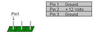
| U8K1 is a Dallas DS12887 real time CMOS battery soldered on the motherboard. |
| U7K1 is the built-in keyboard controller (N82C42PE). |
| J9H1 is a male 2 x 17-pin floppy drive connector. |
| J9H2 is a male 2 x 20-pin ISA/IDE connector. |
| J9G1 is a male 2 x 20-pin PCI/IDE connector. |
| U8B1 through U9D2 comprise the 8 MB (4 MB x 1 x 70) on-board memory. |
 |
| This is the Flash BIOS EEPROM surface mounted on the motherboard. |
 |
 |
| U3L1 is the CL-5434 Cirrus Logic video controller that is built-in on the motherboard. |
| U1J1 and U1L1 make up the 1 MB video memory built-in on the motherboard. |
 |
 |
 |
| J1J1: Cpu Speed | J1J2: Clock Multiplier |
| 1-2: 75MHz Base Cpu Speed | 1-2: 2x Clock Multiplier |
| 2-3: 90MHz Base Cpu Speed | 2-3: 1.5x Clock Multiplier |
| DO NOT CHANGE |
| U4H1 Manfacturer: PCTech, Inc./CMD Technologies Package type: 132-lead PLCC. |
| U1E1 thru U2G2 make up the 256K L2 cache built-in on the motherboard. |
| U4C1 Manufacturer: Intel Corp. Package type: 208-lead QFP |
| U3F1 thru U4E1 Manufacturer: Intel Corp Package type: 208-lead QFP. |
| Note: | Though the PB540, PB550, and PB560 use basically the same motherboard, each uses a different crystal. The differences in speed cannot be changed through jumper setting. Therefore, the CPUs are NOT interchangeable between the three systems [PB540/550/560]. | |||
| PB540 Pentium 75 MHz | ||||
| PB550 Pentium 90 MHz | ||||
| PB560 Pentium 100 MHz | ||||
| Uses the 320-pin Type 5 CPU Zero Insertion Force (ZIF) Socket | ||||
| Not keyboard switchable. | ||||
| Disable cache to slow down the system. | ||||
 |
 |
|
| This capacitor only exist on the PB560 motherboard. |
| These two sockets allow video memory to be upgraded to 2MB from the 1MB that has been integrated with the motherboard. |
| See Also: |
| Video Upgrade Information |
| Note: | Earlier version of the PB550 motherboards have only two SIMM sockets, using socket J5D1 and J6D1. All new releases of the Pentium motherboards [PB540/550/560] have four SIMM sockets, accommodating up to 136 MB of total RAM upgrade. | |
| Standard on motherboard: | 8MB | |
| Maximum on motherboard: | ||
| 2 SIMM Sockets | 72 MB | |
| 4 SIMM Sockets | 136 MB | |
| Maximum addressable: | 4 GB | |
| Uses 1/2/4/8/16/32 MB 72-pin SIMMs, 70ns | ||