Would you like to make this site your homepage? It's fast and easy...
Yes, Please make this my home page!
PB600 Motherboard Layout
Note
Installing a video expansion card will automatically disable
the on board video controller.
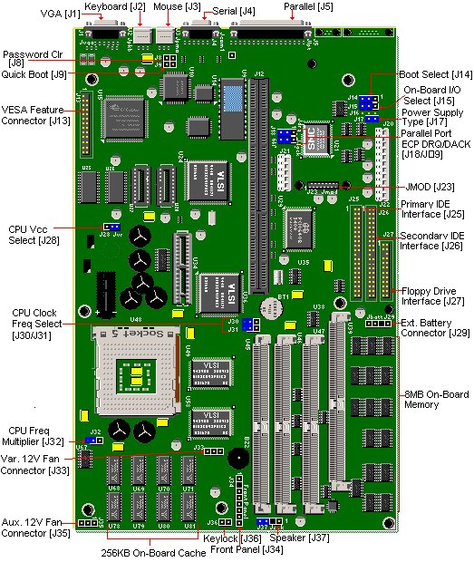
Sockets
Jumpers
Connectors
PB600 Sockets
| U1* | ST7034 |
| U2* | 10BTFILT |
| U3 | 7406 |
| U4 | SN75189A |
| U5 | SN75189A |
| U6 | DS1488M |
| U7 | 74HCT14 |
| U8 | LM3342 |
| U9 | 28F001BX |
| U10 | N8242PC |
| U11 | 28F200BX |
| U12* | SMC91C92 |
| U13* | 93C46AS |
| U14 | PAL16L8-25 |
| U15 | GD543X |
| U16* | 93C46A |
| U17 | 74LS273 |
| U18 | 74LS125 |
| U19 | 74F125 |
| U20 | 74LS125 |
| U21 | 37C665 |
| U22 | 74LS32 |
| U23 | 74LS126 |
| U24 | VL82C593 |
| U25 | 256X16DRM |
| U26 | 256X16DRM |
| U27 | 256X16 SOJ Socket |
| U28 | 256X16 SOJ Socket |
| U29 | PCI0640B |
| U30 | MC34063AS |
| U31 | 74F125 |
| U32 | MC34063A |
| U33 | 8KX8 TAG |
| U34 | 8KX8 TAG |
| U35 | IMI SC471 |
| U36 | VL82C591 |
| U37 | 74F74 |
| U38 | IMI SC471 |
| U39 | SIMM Socket |
| U40 | 1MX4DRAM |
| U41 | 1MX4DRAM |
| U42 | 1MX4DRAM |
| U43 | Not Used |
| U44 | 1MX16DRAM |
| U45 | SIMM Socket |
| U46 | SIMM Socket |
| U47 | SIMM Socket |
| U48 | Socket 5 |
| U49 | VL82C592 |
| U50 | 1MX4DRAM |
| U51 | 1MX4DRAM |
| U52 | 1MX4DRAM |
| U53 | 74F245 |
| U54 | 1MX4DRAM |
| U55 | 1MX4DRAM |
| U56 | 1MX4DRAM |
| U57 | 1MX16DRAM |
| U58 | VL82C592 |
| U59 | 74F245 |
| U60 | 74LS125 |
| U61 | 1MX4DRAM |
| U62 | 1MX4DRAM |
| U63 | 1MX16DRAM |
| U64 | 74F245 |
| U65 | 1MX4DRAM |
| U66 | 1MX4DRAM |
| U67 | 74FCT163374AS |
| U68 | 32KX8SRAM |
| U69 | 32KX8SRAM |
| U70 | 32KX8SRAM |
| U71 | 32KX8SRAM |
| U72 | 1MX4DRAM |
| U73 | 74F245 |
| U74 | 1MX16DRAM |
| U75 | 1MX4DRAM |
| U76 | 1MX4DRAM |
| U77* | 74HCT14 |
| U78 | 32KX8SRAM |
| U79 | 32KX8SRAM |
| U80 | 32KX8SRAM |
| U81 | 32KX8SRAM |
| U82* | GAL16V8F255 |
| U83 | Not Used |
| U84 | PAL20L8-25 |
| Y1* | 20 MHz |
| Y2 | 32.768 MHz |
| Y3 | 14.318 MHz |
*May not be implemented.
PB600 Jumpers
| Jumper | Function | Pin/Setting
| Configuration |
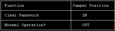
| J8 | Password Clear | In Out (default)
| Clear Password Normal Operation |
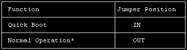
| J9 | Quick Boot | In Out (default)
| Quick Boot Normal Operation |
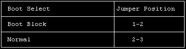
| J14 | Boot Select | 1-2 2-3 (default)
| Boot Block Normal |
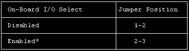
| J15 | On-Board I/O Select |
1-2 2-3 (default) | Disabled Enabled
|
| J16 | Parity Select (Only if no on-board memory)
| 1-2 (default) 2-3 | Parity Check Disabled Parity Check Enabled
|
| J17 | Power Supply Type |
In (default) Out | Standard With Stand-by
|
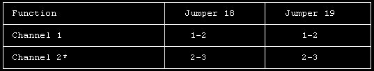
| J18 | Parallel Port ECP DRQ |
1-2 2-3 (default) | Channel 1 Channel 3
|
| J19 | Parallel Port ECP DACK
| 1-2 2-3 (default) | Channel 1 Channel 3
|
| J28 | CPU VCC Select | 1-2 (default) 2-3
| VR (+3.3V) VRE (+3.45V) |
| J29 | Battery | In (default) Out
| On-Board Lithium battery External battery |
| J30 | Host Bus Frequency |
In (default) Out | 60/66 MHz 50 MHz
|
| J31 | Host Bus Frequency |
In Out (default) | 66 MHz 50/60 MHz
|
| J32 | Host Core Frequency Multiplier
| In (default) Out | 2 X - Host Bus Frequency 1.5X - Host Bus Frequency
|
| J37 | Speaker | In (default) Out
| On-Board Speaker External Speaker |
PB600 Connectors
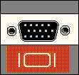
| J1 | VGA Monitor Connector
|
| J2 | PS/2™ Keyboard Connector
|
| J3 | PS/2™ Mouse Connector
|
| J4 | Serial Port (COM 1) Connector
|
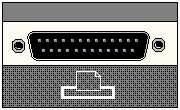
| J5 | Parallel Port Connector
|
| J10 | Boot Block Programming Power Connector
|
| J11 | LAN Expansion Header
|
| J12 | Riser Connector |
| J13 | VESA® Feature Connector
|
| J20 | Primary Power Connector
|
| J21 | Auxiliary Power Connector
|
| J22 | Primary Power Connector
|
| J23 | Internal Header |
| J24 | Infra Red Connector |
| J25 | Primary PCI IDE Connector
|
| J26 | Secondary PCI IDE Connector
|
| J27 | Floppy Connector |
| J33 | Variable 12V Fan Connector |
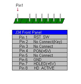
| J34 | Front Panel Connector |
| J35 | Auxiliary 12V Fan Connector
|
| J36 | Keyboard Lock Connector |
J1: Video Port
A female DB15 connector built-in on the motherboard.
J5: Parallel Port
A female DB25 connector built-in on the motherboard.
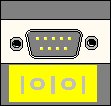
J4: External Serial Port
A male DB9 connector built-in on the
motherboard.
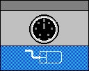
J3: PS/2 Mouse Port
A female 6-pin mini DIN connector built-in
on the motherboard.
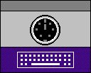
J2: PS/2 Keyboard Port
A female 6-pin mini DIN connector built-in
on the motherboard.
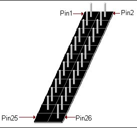
J12: Riser Card Connector
This riser can accommodate the following expansion slots configuration:
4 X 4 Case 2 ISA slots 1 PCI slot 1 Combo PCI/ISA slot Mini Tower
2 ISA slots 2 PCI slot 1 Combo PCI/ISA slot
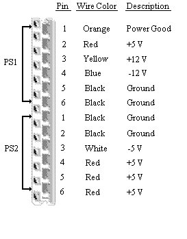
J20/J22: Power Connector (PS1 / PS2)
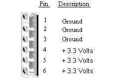
J21: PCI Bus Power Connector
This is the 3.3V Power Connector for the PCI bus.
U25/U26: Video Memory
These two chips make up the 1 MB video memory built-in on the
motherboard.
See Also:
VIDEO UPGRADE INFORMATION
U15: Cirrus Logic Video Chipset
The Cirrus Logic GD-5430 video
controller is soldered onto the motherboard.
J13: Video Feature Connector
J13 is a male 2 x 13-pin VESA feature connector allowing
video to be routed through a video capture card or a PBTV card.
J27: Floppy Drive Interface
J27 is a male 2 x 17-pin floppy drive connector. Capable of supporting
up to 2.88 MB capacity floppy drive
J25: Primary Hard Drive
Interface This male 2 x 20-pin connector is the primary IDE interface.
BIOS supports for: Type F DMA and AT API Devices Logical Block
Addressing (LBA) Enhance CHS Capable of supporting up to PIO Mode 3
J26: Secondary Hard Drive Interface
This male 2 x 20-pin connector
is the secondary IDE interface. BIOS supports for: Type F DMA
and AT API Devices Logical Block Addressing (LBA) Enhance CHS
Capable of supporting up to PIO Mode 3
BT1: Battery
This 3V
Lithium battery is permanently soldered on the motherboard at
location BT1. See Also:
BATTERY UPGRADE INFORMATION
U27/U28: Video Memory Upgrade Socket
Sockets U27 and U28 will allow video
memory to be upgraded to 2MB from the 1MB that has been integrated
with the motherboard.See Also:
VIDEO UPGRADE INFORMATION
U48: CPU Socket
This is the CPU socket. This CPU socket can accommodate
any of the following CPUs
Intel Pentium 75 MHz Intel Pentium 120
MHz Intel Pentium 90 MHz Intel Pentium 133 MHz Intel Pentium 100
MHz Uses Zero Insertion Force (ZIF) socket Uses the 320-pin Type
5 CPU Socket Not keyboard switchable. Disable cache to slow down
system. See Also:
PROCESSOR UPGRADE INFORMATION
RAM Memory Upgrade Socket
SOCKET ORIENTATION: The socket closest to the CPU (leftmost
socket) is U45, and the one right next to it to the right is U46.
These two sockets make up the second bank (BANK 3). The next one
over to the right is socket U47, and the right most socket is
U39. These two sockets make up the first bank (BANK 2). This motherboard
uses one vertical right key (U45) and three angled (22 degree)
left key metal latch SIMM sockets.
See Also:
RAM UPGRADE INFORMATION
On-Board RAM Memory
The system comes generally with 8 MB of
memory soldered on board.
NOTE:
Some PB600 systems do NOT have
any RAM soldered on board See Also:
RAM UPGRADE INFORMATION
U11: Flash BIOS
This makes it possible for the BIOS to be upgraded
via software rather than replacing the BIOS chip.
See Also:
BIOS UPGRADE INFORMATION
External Cache
This motherboard comes with 256KB L2 (external) cache soldered
on-board located at: U67, U68, U69, U70, U71, U78, U79, U80, U81.
NOTE:
(Not all systems come with 256K L2 cache)
J8: Password Clear
J9: Quick Boot
J14: Boot Select
J15: On-Board I/O Select
J16: Parity Select
(Only if No on-board
memory) This is only a trace.
J17: Power Supply Type
"This jumper is reserved. Do not change."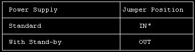
J18/J19: Parallel Port ECP DRQ/DACK
J28: CPU VCC Select
"Caution: do not change this jumper. Reserved for
future use."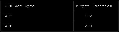
J29: Battery Select
"The external battery
connects to pins 1 and 4 after the jumper between pins 3 and 4
is removed."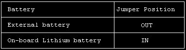
See Also:
BATTERY UPGRADE INFORMATION
J30/J31: CPU Clock Frequency Select
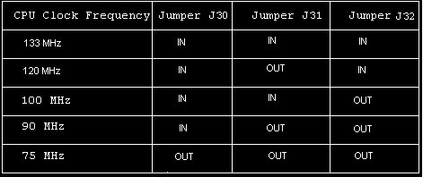
J32: CPU Core Frequency Multiplier (Alt. CPU ONLY)
U34: Tag RAM Socket
Reserved for development testing only. Not implemented.
J34: Front Panel Connector