|
|
|

Location | Description |
| U1J2 | P58AN-CD4052BCM National |
| U1J1 | 317MB-QF528 Motorola |
| U2J1 | 9559 C USA-MT4C1627ODJ -5 |
| U3J1 | 9559 C USA-MT4C1627ODJ -5 |
| U3J2 | 9559 C USA-MT4C1627ODJ -5 |
| U4J1 | 9559 C USA-MT4C1627ODJ -5 |
| U5J1 | 62A52RT-GD75232 TI |
| U9C1 | P61SP-74F125 National |
| U8B1 | FS95G2KBE4- PC87306-IBQ/VUL National |
| U9A1 | EX28F002-BXT80 Intel |
| U8C1 | 74F08D-FWR4163-9609nN |
| U8B2 | 74ALS00AD-9609nE |
| U8A2 | F2245-63k-CT9Y |
| U8A1 | 74F08D-FWR4163-9609nN |
| U7A2 | 74HCT14D-V8I25HME-crn9609 |
| U7A4 | F2245-63k-CT9Y |
| U7A1 | 64CNF3K-7407 |
| U7A3 | 43IBC-XCOL |
| U6A2 | TC4427-COA |
| U6A3 | LM393A-5AT |
| U6A1 | 606-NDS-9410a |
| U5A1 | 606-NDS-9410a |
| U6C1 | PCIset SB82371SB Intel |
| U5C1 | PCIset SB82437VX Intel |
| U4D1 | W24M257AJ-15 95271 Winbond |
| U3C1 | Socket 7 |
| U1B1 | 74ALS00AD-9609Ne |
| U1E1 | ICS9169M 9612-03 |
| U2E1 | Sony CXK77V321Q-14 610AT7E S |
| U2F1 | Sony CXK77V321Q-14 610AT7E S |
| U4E1 | PCIset S82438VX |
| U4F1 | PCIset S82438VX |
| U2G1 | 63CKNEK 7406 |
| U2H1 | Bt829KPF Video Decoder |
| U4H1 | S3 Virge H1C3BB |
Function | Location | Jumpers | Configuration |
| Host Bus Speed | J1F2C | 1-2, 5-6 | 66MHz |
| (note: PCI clock speed | 2-3, 4-5 | 60MHz | |
| equals ½ Host bus speed) | 2-3, 5-6 | 50MHz | |
| CPU Clock Ratio | J1F2D | 1-2, 4-5 | x1.5 |
| 2-3, 4-5 | x2.0 | ||
| 2-3, 5-6 | x2.5 | ||
| 1-2, 5-6 | x3.0 | ||
| CMOS Clear | J1F2A | 4-5 | Normal |
| 5-6 | Clear | ||
| Password Clear | J1F2A | 1-2 | Password Enabled |
| 2-3 | Password Disabled | ||
| CMOS Setup Access | J1F2B | 1-2 | Enabled |
| 2-3 | Access Denied | ||
| Processor Voltage | J1F2B | 4-5 | Standard Voltage (3.3v) |
| 5-6 | VRE | ||
| Recovery Mode | J9C1 | 1-2 | Normal |
| 2-3 | Recovery | ||
| 4-5, 5-6 | Reserved |
Connector | Description |
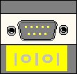
| J9L1 | Serial Port |
| J7L1 | Parallel Port |
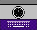
| J6L1 | PS/2™ Keyboard Connector |
| J5L1 | PS/2™ Mouse Connector |
| J3L1 | I2C Port and S-Video |
| J2L1 | RCA Connector |
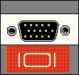
| J1L1 | VGA Monitor Connector |
| J8E1 | Primary PCI IDE Connector |
| J9E1 | Secondary PCI IDE Connector |
| J8G1 | Floppy Connector |
| J1H1 | VESA Feature Connector |
| J9E2 | Primary Power Connector |
| J9G2 | 3.3v Power Connector |
| J6G1 | Riser Connector |
| J6F1 | SIMM Socket - Bank 0 |
| J7F1 | SIMM Socket - Bank 0 |
| J7F2 | SIMM Socket - Bank 1 |
| J8F1 | SIMM Socket - Bank 1 |
| J1L1 | Video Memory Connector |
| J4l2 | Video Memory Connector |
| J8K1 | CD Audio Reserved |
| J9J1 | Midi/Audio Reserved |
| J9N2 | Line-Out Package |
| J8N2 | Microphone-In Package |
| J9J2 | Wave-Table Reserved |
| J2A1 | Internal Speaker |


| 4 X 4 Case: | 2 ISA slots 1 PCI slot 1 Combo PCI/ISA slot |
| Mini Tower: | 2 ISA slots 2 PCI slots 1 Combo PCI/ISA slot |


Function |
Jumpers |
Configuration |
| CMOS Clear | J1F2A | 4-5 - Normal 5-6 - Clear |
| Password Clear | J1F2A | 1-2 - Password Enabled 2-3 - Password Disabled |
| CMOS Setup Access | J1F2B | 1-2 - Enabled 2-3 - Access Denied |
| Processor Voltage | J1F2B | 4-5 - Standard Voltage (3.3v) 5-6 VRE |
| Host Bus Speed, (Note: PCI clock speed equals1/2 Host Bus Speed) |
J1F2C | 1-2, 5-6 - 66 MHz 2-3, 4-5 - 60 MHz 2-3, 5-6 - 50 MHz |
| CPU Clock Ratio | J1F2D | 1-2, 4-5 - x1.5 2-3, 4-5 - x2.0 2-3, 5-6 - x2.5 1-2, 5-6 - x3.0 |

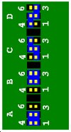
Pin# |
Signal |
| 1. | Negative |
| 2. | Positive |
Pin# |
Signal |
| 1. | Negative (Black) |
| 2. | Positive (Red) |
| 3. | No Connection |

Pin# |
Signal |
| 1. | a. Gnd |
| 2. | a. Gnd |
| 3. | y (luma) |
| 4. | c (chroma) |
| 5. | sck (i2c) |
| 6. | +12v |
| 7. | sda (i2c ) |