|
|
|

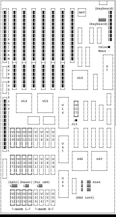
2. REV-D motherboard holds 2MB of RAM. Each Megabyte is (8) 256k
x 4 and (4) 256k x 1 chips for parity.
Socket |
Chip |
Description |
| U7 | 8042 | Keyboard Controller |
| U10 | 83C206 | |
| U14 | 82C212 or 82C212B | |
| U15 | 80286 | Main Processor |
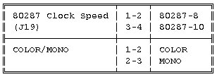
| U16 | 80287 | Math Coprocessor (optional) |
| U17 | 30-32MHZ | Crystal (optional) |
| U47 | BIOS (High) | |
| U69 | BIOS (Low) | |
| U48 | 82C215 | |
| U49 | 82C211C |