|
|
|
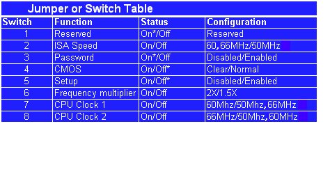
| Switch | Function | Status | Configuration |
|---|---|---|---|
| 1 | Reserved | On* Off |
Reserved |
| 2 | ISA Speed | On Off |
60 or 66 MHz 50 MHz |
| 3 | Password | On* Off |
Disabled Enabled |
| 4 | CMOS | On Off* |
Clear Normal |
| 5 | Setup | On Off* |
Disabled Enabled |
| 6 | Frequency Multiplier | On Off |
2X 1.5X |
| 7 | CPU Clock 1 | On Off |
60 MHz 50 or 66 MHz |
| 8 | CPU Clock 0 | On Off |
66 MHz 50 or 60 MHz |
Jumper |
Function/Jumped |
Status |
Configuration/Jumped |
| J13J1 | Reserved - CPU Voltage | 1-2 2-3 |
VR VRE |
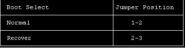
| J26 | BIOS Recovery | 1-2 2-3 |
Normal Recovery Mode |
Note
Some configurations of this series of motherboards may list the BIOS Recovery Jumper as J5A2. Both designations are valid. The jumper is in the same location and the settings are the same.
Jumper |
Description |
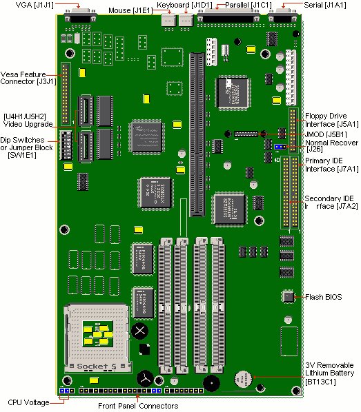
| J1A1 | Serial Port Connector |
| J1C1 | Parallel Port Connector |
| J1D1 | PS/2™ Keyboard Connector |
| J1E1 | PS/2™ Mouse Connector |
| J1J1 | VGA Monitor Connector |
| J7A1 | Primary PCI IDE Connectors |
| J7A2 | Secondary PCI IDE Connectors |
| J5A1 | Floppy Connector |
| J4D1 | Riser Connector |
| J10D1 | SIMM Sockets- Bank 1 |
| J10D2 | SIMM Sockets- Bank 1 |
| J10E1 | SIMM Sockets- Bank 0 |
| J10F1 | SIMM Sockets- Bank 0 |
| J5B1 | Daughter Board Connector |
| J3J1 | VESA® Feature Connector |
| J2A1 | Primary Power Connector |
| J2D1 | Auxiliary 3.3V Connector |
| U4H1 | SOJ Video Memory Sockets |
| U5H2 | SOJ Video Memory Sockets |
| J13H1 | Front Panel Connectors |
| J13F1 | Front Panel Connectors |
J1J1: Video Port |
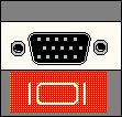 |
| A female DB15 Connector built-in on the motherboard. |
J1C1: Parallel Port |
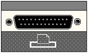 |
| A female DB25 Connector built-in on the motherboard. |
J1A1: External Serial Port |
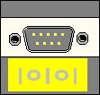 |
| A male DB9 Connector built-in on the motherboard. |
J1E1: PS/2 Mouse Port |
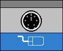 |
| A female 6-pin mini DIN Connector built-in on the motherboard. |
J1D1: PS/2 Keyboard Port |
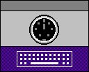 |
| A female 6-pin mini DIN Connector built-in on the motherboard. |
J4D1: Riser Card Connector |
||
4 X 4 Case | 2 ISA slots | |
| 1 PCI slot | ||
| 1 Combo PCI/ISA slot | ||
Mini Tower | 2 ISA slots | |
| 2 PCI slot | ||
| 1 Combo PCI/ISA slot |
J5B1: Daughterboard Modem Connector |
| A 20-pin Connector normally referred to as the JMOD Connector. |
J2A1: Power Connector |
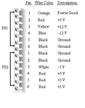 |
J2D1: PCI Bus Power Connector |
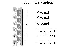 |
| This is the 3.3V Power Connector for the PCI bus. |
J26: BIOS Recovery |
 |
U4H2, U5H1: Video Memory |
| These two chips make up the 1 MB video memory built-in on the motherboard. See Also Video Upgrade Information. |
U4F1: Cirrus Logic Video Chipset |
| This is the Cirrus Logic GD-5430 video controller that is built-in on the motherboard. See Also Video Upgrade Information. |
J3J1: Video Feature Connector |
 |
J5A1: Floppy Drive Interface |
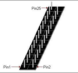
| J9H1 is a male 2 x 17-pin floppy drive Connector. Capable of supporting up to 2.88 MB capacity floppy drive. |
J7A1: Primary Hard Drive Interface |
| This male 2 x 20-pin Connector is the primary IDE interface. |
| BIOS supports for |
| Type F DMA and AT API Devices |
| Logical Block Addressing (LBA) |
| Enhance CHS |
| Capable of supporting PIO Mode 3 and Mode 4 |
J7A2: Secondary Hard Drive Interface |
| This male 2 x 20-pin Connector is the secondary IDE interface. |
| BIOS supports for |
| Type F DMA and AT API Devices |
| Logical Block Addressing (LBA) |
| Enhance CHS |
| Capable of supporting PIO Mode 3 and Mode 4 |
BT13C1: Battery |
| This is the clip-in 3V replaceable Lithium battery. |
| It uses a 3V CR2032 battery. |
SW1E1: Dip Switches or Jumper Block |
|
| Note The following dip switch setting tables have been printed on the motherboard as well, towards the front of the video upgrade sockets. Some motherboards have a jumper block instead of dip switches. The settings are the same as those for the dip switches. |
 |
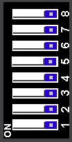
| Note The settings with * are the default setting. |
 |
U4H1/U5H2: Memory Upgrade Socket |
| These two sockets allow video memory to be upgraded to 2MB from the 1MB that has been integrated with the motherboard. See Also Video Upgrade Information |
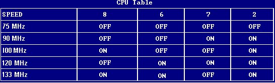
U11H1: CPU Socket |
| This is the CPU socket. This CPU socket can accomodate any of the following CPUs |
| Switch 6 Position | |||
| Intel Pentium 75 MHz | OFF | ||
| Intel Pentium 90 MHz | OFF | ||
| Intel Pentium 100 Mhz | OFF | ||
| Intel Pentium 120 Mhz | ON | ||
| Intel Pentium 133 Mhz | ON | ||
| Uses 320-pin Type 5 CPU Zero Insertion Force (ZIF) socket | |||
| Uses the Socket | |||
| Not keyboard switchable. | |||
| Disable cache to slow down the system. | |||
| See Also Processor Upgrade Information | |||
Memory Upgrade Socket |
Note |
| This motherboard does not have any built-in memory. However, the system is usually shipped with 8MB of EDO memory, taking up the first bank (BANK 0) with two 4MB SIMMs. |
Socket Orientation |
| The socket closest to the CPU (leftmost socket) is J10F1, and the one right next to it to the right is J10E1. These two sockets make up the first bank (BANK 0). The next one over to the right is socket J10D2, and the right most socket is J10D1. These two sockets make up the second bank (BANK 1). See Also Ram Upgrade Information |
Flash BIOS |
| The Intel N28F001BXT is the 1Mb Flash BIOS chip (128KB) used with this motherboard. |
| This allow for the BIOS to be upgraded via software rather than replacing the BIOS chip itself. |
CPU Voltage Jumper |
| This jumper sets the CPU voltage from 3.3v to variable voltage. Default Setting 1-2. |
Note |
| Changing setting may result in motherboard damage. |
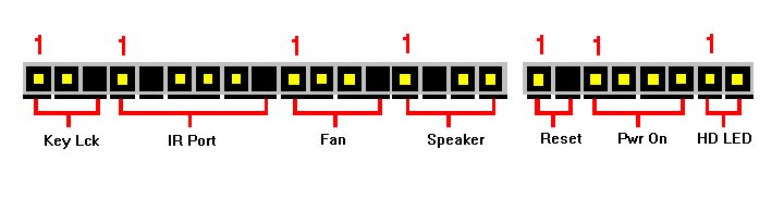
PB570 Motherboard Front Panel Connectors |
| Connectors for front panel functions. Connector blocks J13H1 and J13F1 Front Panel Connectors. |